Saturday 2 November 2019

Don’t Care (X) Conditions in K-Maps

Don’t Care (X) Conditions in K-Maps

The “Don’t Care” conditions allow us to replace the empty cell of a K-Map to form a grouping of the variables. While forming groups of cells, we can consider a “Don’t Care” cell as either 1 or 0 or we can simply ignore that cell. Therefore, “Don’t Care” condition can help us to form a larger group of cells.
A Don’t Care cell can be represented by a cross(X) in K-Maps representing a invalid combination. For example, in Excess-3 code system, the states 0000, 0001, 0010, 1101, 1110 and 1111 are invalid or unspecified. These are called don’t cares. Also, in design of 4-bit BCD-to-XS-3 code converter, the input combinations 1010, 1011, 1100, 1101, 1110, and 1111 are don’t cares.
A standard SOP function having don’t cares can be converted into a POS expression by keeping don’t cares as they are, and writing the missing minterms of the SOP form as the maxterm of POS form. Similarly, a POS function having don’t cares can be converted to SOP form keeping the don’t cares as they are and write the missing maxterms of the POS expression as the minterms of SOP expression.
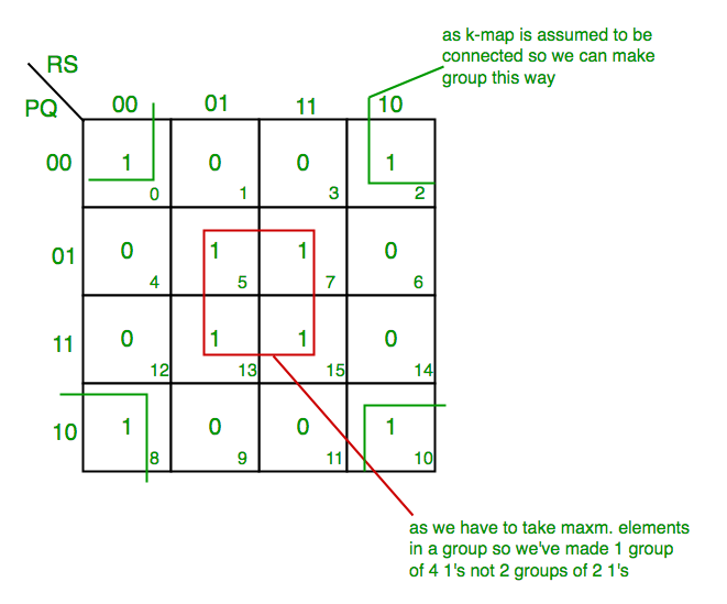

Example-1:
Minimise the following function in SOP minimal form using K-Maps:
f = m(1, 5, 6, 12, 13, 14) + d(4) 
Explanation:
The SOP K-map for the given expression is:
Therefore, SOP minimal is,
f = BC' + BD' + A'C'D 
Example-2:
Minimise the following function in SOP minimal form using K-Maps:
F(A, B, C, D) = m(0, 1, 2, 3, 4, 5) + d(10, 11, 12, 13, 14, 15) 
Explanation:
Writing the given expression in POS form:
F(A, B, C, D) = M(6, 7, 8, 9) + d(10, 11, 12, 13, 14, 15) 
The POS K-map for the given expression is:
Therefore, POS minimal is,

F = A'(B' + C') 
Example-3:
Minimise the following function in SOP minimal form using K-Maps: F(A, B, C, D) = m(1, 2, 6, 7, 8, 13, 14, 15) + d(3, 5, 12)
Explanation:
The SOP K-map for the given expression is:
Therefore,
f = AC'D' + A'D + A'C + AB 
Significance of “Don’t Care” Conditions:
Don’t Care conditions has the following significance with respect to the digital circuit design:
  1. Simplification:
    These conditions denotes the set of inputs which never occurs for a given digital circuits. Thus, they are being used to further simplify the boolean output expression.
  2. Lesser number of gates:
    Simplification reduces the number of gates to be used for implementing the given expression. Therefore, don’t cares make the digital circuit design more economical.
  3. Reduced Power Consumption:
    While grouping the terms long with don’t cares reduces switching of the states. This decreases the required memory space which in turn results in less power consumption.
  4. States in Code Converters:
    These are used in code converters. For example- In design of 4-bit BCD-to-XS-3 code converter, the input combinations 1010, 1011, 1100, 1101, 1110, and 1111 are don’t cares.
  5. Prevention of Hazards:
    Don’t cares also prevents hazards in digital systems.

K-Map (Karnaugh Map)

K-Map (Karnaugh Map)


In many digital circuits and practical problems we need to find expression with minimum variables. We can minimize Boolean expressions of 3, 4 variables very easily using K-map without using any Boolean algebra theorems. K-map can take two forms Sum of Product (SOP) and Product of Sum (POS) according to the need of problem. K-map is table like representation but it gives more information than TRUTH TABLE. We fill grid of K-map with 0’s and 1’s then solve it by making groups.
Steps to solve expression using K-map-
  1. Select K-map according to the number of variables.
  2. Identify minterms or maxterms as given in problem.
  3. For SOP put 1’s in blocks of K-map respective to the minterms (0’s elsewhere).
  4. For POS put 0’s in blocks of K-map respective to the maxterms(1’s elsewhere).
  5. Make rectangular groups containing total terms in power of two like 2,4,8 ..(except 1) and try to cover as many elements as you can in one group.
  6. From the groups made in step 5 find the product terms and sum them up for SOP form.

SOP FORM

  1. K-map of 3 variables-
Z= ∑A,B,C(1,3,6,7)

de1

From red group we get product term—
A’C
From green group we get product term—
AB
Summing these product terms  we get- Final expression (A’C+AB)
  1. K-map for 4 variables
F(P,Q,R,S)=∑(0,2,5,7,8,10,13,15)

de2

From red group we get product term—
QS
From green group we get product term—
Q’S’

Summing  these product terms  we get- Final expression (QS+Q’S’)

Digital logic | Shift Registers


Digital logic | Shift Registers


Flip flops can be used to store a single bit of binary data (1or 0). However, in order to store multiple bits of data, we need multiple flip flops. N flip flops are to be connected in an order to store n bits of data. A Register is a device which is used to store such information. It is a group of flip flops connected in series used to store multiple bits of data.
The information stored within these registers can be transferred with the help of shift registers. Shift Register is a group of flip flops used to store multiple bits of data. The bits stored in such registers can be made to move within the registers and in/out of the registers by applying clock pulses. An n-bit shift register can be formed by connecting n flip-flops where each flip flop stores a single bit of data.
The registers which will shift the bits to left are called “Shift left registers”.
The registers which will shift the bits to right are called “Shift right registers”.
Shift registers are basically of 4 types. These are:
1.Serial In Serial Out shift register
Serial In parallel Out shift register
Parallel In Serial Out shift register
Parallel In parallel Out shift register

Serial-In Serial-Out Shift Register (SISO) –

The shift register, which allows serial input (one bit after the other through a single data line) and produces a serial output is known as Serial-In Serial-Out shift register. Since there is only one output, the data leaves the shift register one bit at a time in a serial pattern, thus the name Serial-In Serial-Out Shift Register.
The logic circuit given below shows a serial-in serial-out shift register. The circuit consists of four D flip-flops which are connected in a serial manner. All these flip-flops are synchronous with each other since the same clock signal is applied to each flip flop.
The above circuit is an example of shift right register, taking the serial data input from the left side of the flip flop. The main use of a SISO is to act as a delay element.

Serial-In Parallel-Out shift Register (SIPO) –

The shift register, which allows serial input (one bit after the other through a single data line) and produces a parallel output is known as Serial-In Parallel-Out shift register.
The logic circuit given below shows a serial-in-parallel-out shift register. The circuit consists of four D flip-flops which are connected. The clear (CLR) signal is connected in addition to the clock signal to all the 4 flip flops in order to RESET them. The output of the first flip flop is connected to the input of the next flip flop and so on. All these flip-flops are synchronous with each other since the same clock signal is applied to each flip flop.
The above circuit is an example of shift right register, taking the serial data input from the left side of the flip flop and producing a parallel output. They are used in communication lines where demultiplexing of a data line into several parallel lines is required because the main use of the SIPO register is to convert serial data into parallel data.

Parallel-In Serial-Out Shift Register (PISO) –

The shift register, which allows parallel input (data is given separately to each flip flop and in a simultaneous manner) and produces a serial output is known as Parallel-In Serial-Out shift register.
The logic circuit given below shows a parallel-in-serial-out shift register. The circuit consists of four D flip-flops which are connected. The clock input is directly connected to all the flip flops but the input data is connected individually to each flip flop through a multiplexer at the input of every flip flop. The output of the previous flip flop and parallel data input are connected to the input of the MUX and the output of MUX is connected to the next flip flop. All these flip-flops are synchronous with each other since the same clock signal is applied to each flip flop.
A Parallel in Serial out (PISO) shift register us used to convert parallel data to serial data.

Parallel-In Parallel-Out Shift Register (PIPO) –

The shift register, which allows parallel input (data is given separately to each flip flop and in a simultaneous manner) and also produces a parallel output is known as Parallel-In parallel-Out shift register.
The logic circuit given below shows a parallel-in-parallel-out shift register. The circuit consists of four D flip-flops which are connected. The clear (CLR) signal and clock signals are connected to all the 4 flip flops. In this type of register, there are no interconnections between the individual flip-flops since no serial shifting of the data is required. Data is given as input separately for each flip flop and in the same way, output also collected individually from each flip flop.
A Parallel in Parallel out (PIPO) shift register is used as a temporary storage device and like SISO Shift register it acts as a delay element.

Differences between Synchronous and Asynchronous Counter


  1. Differences between Synchronous and Asynchronous Counter


Counters are of two types depending upon clock pulse applied. These counters are: Asynchronous counter, and Synchronous counter.
In Asynchronous Counter is also known as Ripple Counter, different flip flops are triggered with different clock, not simultaneously. While in Synchronous Counter, all flip flops are triggered with same clock simultaneously and Synchronous Counter is faster than asynchronous counter in operation.
Let’s see the difference between these two counters:
S.NOSynchronous CounterAsynchronous Counter
1.In synchronous counter, all flip flops are triggered with same clock simultaneously.In asynchronous counter, different flip flops are triggered with different clock, not simultaneously.
2.


Synchronous Counter is faster than asynchronous counter in operation.


Asynchronous Counter is slower than synchronous counter in operation.
3.Synchronous Counter does not
 produce any decoding errors.
Asynchronous Counter produces decoding error.
4.


Synchronous Counter is also called Serial Counter.


Asynchronous Counter is also called Parallel Counter.
5.


Synchronous Counter designing as well implementation are complex due to increasing the number of states.
Asynchronous Counter designing as well as implementation is very easy.
6.


Synchronous Counter will operate in any desired count sequence.
Asynchronous Counter will operate only in fixed count sequence (UP/DOWN).
7.


Synchronous Counter examples are: Ring counterJohnson counter.
Asynchronous Counter examples are: Ripple UP counter, Ripple DOWN counter